- 您现在的位置:买卖IC网 > Sheet目录320 > DK-DSP-3C120N (Altera)KIT DEV DSP CYCLONE III EDITION
Development Kits
Altera and Partner Development Kits
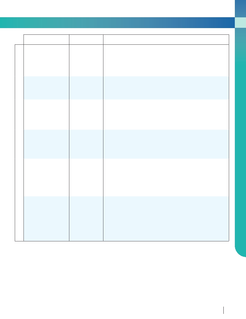
Product and Vendor Name
MAX II/MAX IIZ
Development Kit
System Level Solutions
MAX V CPLD
Development Kit
Altera
CoreCommander
Development Kit
System Level Solutions
Cyclone III LS FPGA
Development Kit
Altera
HSMC Prototyping Board
Bitec
ProcPAK II
GiDEL
Device
MAX II
EPM240
EPM240Z
MAX V 5M570Z
Cyclone III
EP3C25F256C8
Cyclone III LS
EP3CLS200F780C7N
Daughtercard
Cyclone II
EP2C35
Description
This board provides a hardware platform for designing and developing simple and
low-end systems based on Altera MAX II/MAX IIZ devices. The board features a MAX II/
MAX IIZ EPM240T100Cx/EPM240ZM100Cx device with 240 LEs and 8,192 bits of user
flash memory (UFM). The board also supports vertical migration into EPM570T100Cx
devices with 570 LEs and 8,192 bits of UFM.
This low-cost platform will help you quickly begin developing low-cost, low-power
CPLD designs. Use this kit as a stand-alone board or combined with a wide variety of
daughtercards that are available from third parties.
This kit features the Altera Cyclone III FPGA that provides more than enough room for
almost any embedded design. This flexible board comes with a suite of SLS IP Cores,
drivers, and application software. Delivered as a complete package, this kit ensures
quick and easy implementation of industry-leading cores with reduced risk, at a very
low cost.
This kit combines a high-density, low-power Cyclone III LS FPGA with a complete suite
of security features implemented at the silicon, software, and IP levels. These security
features provide passive and active protection of your IP from tampering, reverse
engineering, and counterfeiting. It uses the EP3CLS200 FPGA — 200K LEs at less than
0.25 W static power.
This board provides a solution for prototyping circuits and testing them together with
the latest Altera FPGA development kits. This board provides access to the complete set
of HSMC signals via a footprint of standard 0.1” pitch headers. The HSMC power pins
are accessed via fuses for added security. The main prototype matrix comprises a 0.1”
grid interleaved with +3.3 V and GND access points. Footprints for commonly used 25-
way and 9-way D-type connectors are included on the board.
ProcPAK II development kit is based on Altera’s Stratix II FPGA platform. The
development kit greatly improves time to market. There is no need to design the board,
the PCI driver, or the application driver layer, define board constraints, design memory
controller, and write environment FPGA code. This kit enables designers to focus on
their proprietary value-added design instead of spending their valuable effort to
recreate standard design components. With ProcMultiPort innovative memory
controller, the generated HDL code enables high-speed, easy-to-use parallel access to
large memories.
Altera Product Catalog
?
2013
?
www.altera.com
81
发布紧急采购,3分钟左右您将得到回复。
相关PDF资料
DK-K7-CONN-CES-G
KINTEX-7 FPGA CONNECTIVITY KIT
DK-K7-EMBD-CES-G-J
KINTEX-7 FPGA EMBEDDED KIT JAPAN
DK-MAXII-1270N
KIT DEV MAXII W/EPM 1270N
DK-N2EVAL-3C25N
KIT DEV NIOS II CYCLONE III ED.
DK-NIOS-2C35N
NIOS II KIT W/CYCLONE II EP2C35N
DK-NIOS-2S60N
NIOS II KIT W/STRATIX II EP2S60N
DK-PCI-2C35N
PCI KIT W/CYCLONE II EP2C35N
DK-PCIE-2SGX90N
PCIE KIT W/S II GX EP2SGX90N
相关代理商/技术参数
DK-DSP-3SL150N
功能描述:可编程逻辑 IC 开发工具 FPGA Development Kit For EP3SL150F1152
RoHS:否 制造商:Altera Corporation 产品:Development Kits 类型:FPGA 工具用于评估:5CEFA7F3 接口类型: 工作电源电压:
DK-DTK-120HW
制造商:FLORIDA MISC. 功能描述:
DKE10
制造商:MEANWELL 制造商全称:Mean Well Enterprises Co., Ltd. 功能描述:10W DC-DC Regulated Dual Output Converter
DKE10A-05
功能描述:DC/DC转换器 9-18Vin +/-5Vout 100-1000mA, 10W RoHS:否 制造商:Murata 产品: 输出功率: 输入电压范围:3.6 V to 5.5 V 输入电压(标称): 输出端数量:1 输出电压(通道 1):3.3 V 输出电流(通道 1):600 mA 输出电压(通道 2): 输出电流(通道 2): 安装风格:SMD/SMT 封装 / 箱体尺寸:
DKE10A-12
功能描述:DC/DC转换器 9-18Vin +/-12Vout 42-420mA, 10W RoHS:否 制造商:Murata 产品: 输出功率: 输入电压范围:3.6 V to 5.5 V 输入电压(标称): 输出端数量:1 输出电压(通道 1):3.3 V 输出电流(通道 1):600 mA 输出电压(通道 2): 输出电流(通道 2): 安装风格:SMD/SMT 封装 / 箱体尺寸:
DKE10A-15
功能描述:DC/DC转换器 9-18Vin +/-15Vout 33.3-333mA, 10W RoHS:否 制造商:Murata 产品: 输出功率: 输入电压范围:3.6 V to 5.5 V 输入电压(标称): 输出端数量:1 输出电压(通道 1):3.3 V 输出电流(通道 1):600 mA 输出电压(通道 2): 输出电流(通道 2): 安装风格:SMD/SMT 封装 / 箱体尺寸:
DKE-10A-24
功能描述:DC/DC转换器 10W +/-24V 9-18VDC Dual Output DC-DC RoHS:否 制造商:Murata 产品: 输出功率: 输入电压范围:3.6 V to 5.5 V 输入电压(标称): 输出端数量:1 输出电压(通道 1):3.3 V 输出电流(通道 1):600 mA 输出电压(通道 2): 输出电流(通道 2): 安装风格:SMD/SMT 封装 / 箱体尺寸:
DKE10A-24
制造商:Mean Well 功能描述:DKE10 Series 10 W Dual Output 24 V / -24 V DC/DC Converter Power Supply 制造商:Mean Well 功能描述:Module DC-DC 2 Output 24 Volt-24 Volt 0.21A/-0.21A 10W 5-Pin 制造商:Mean Well 功能描述:Module DC-DC 2-OUT 24V/-24V 0.21A/-0.21A 10W 5-Pin 制造商:Mean Well 功能描述:D/D Module,DC/DC,Module Type,
